Soc Solution
SoC Design Solution
01
SoC Design
02
SoC Verification
03
SoC FPGA prototype
SoC Solution
SoC Solution
RTL Design, Platform Design & Verification, FPGA Verification 부터
Design Service 분야의 DFT Insertion, Layout, PKG / Test까지
시스템반도체 개발 및 제작에 필요한 모든 솔루션을 제공합니다.
Our Skills
Design Service Flow
스펙 협의부터 파운드리 공정 웨이퍼, 칩 아웃까지 턴키 서비스 기술 및 design flow 노하우
STEP 1
Spec. Decision RTL Coding
STEP 2
Synthesis
STEP 3
Netlist Hand-off
STEP 4
DFT Service
STEP 5
Placement Routing
STEP 6
Verification & PG
STEP 7
Test Vector Generation
STEP 8
Failure Analysis
Flow
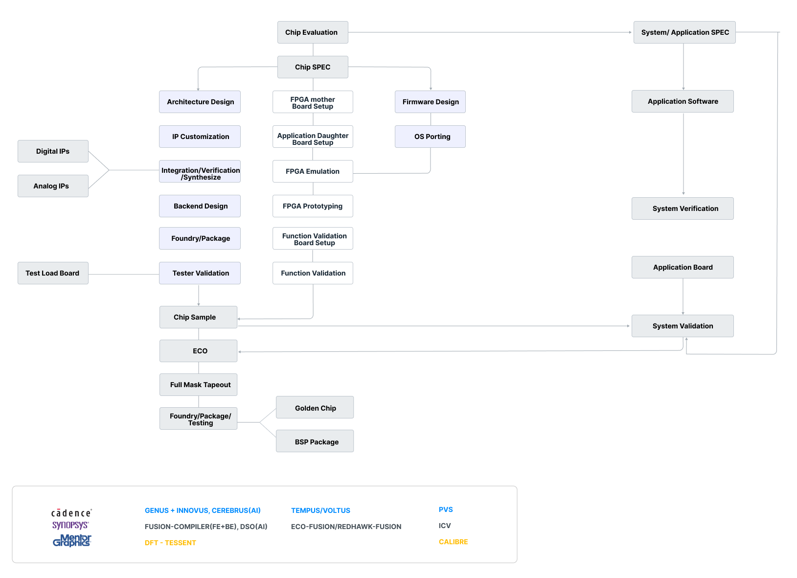
LET'S SoC flow
- ARM-based SoC System : Ready for Entry-to-Cutting Edge
- 3rd Party IP with Partnership
- Early Start and Fast Optimization
SoC System Platform
- Systematic Configured & Re-usable Environment
- All Verification Cases from Top to Sub in One Environment
- Configurable Alternative Models for Integrated Units
- Light and Reliable against Integration Issue
- Easy Porting your System into One Verification Env.
SoC Verification Platform


