Total Solution
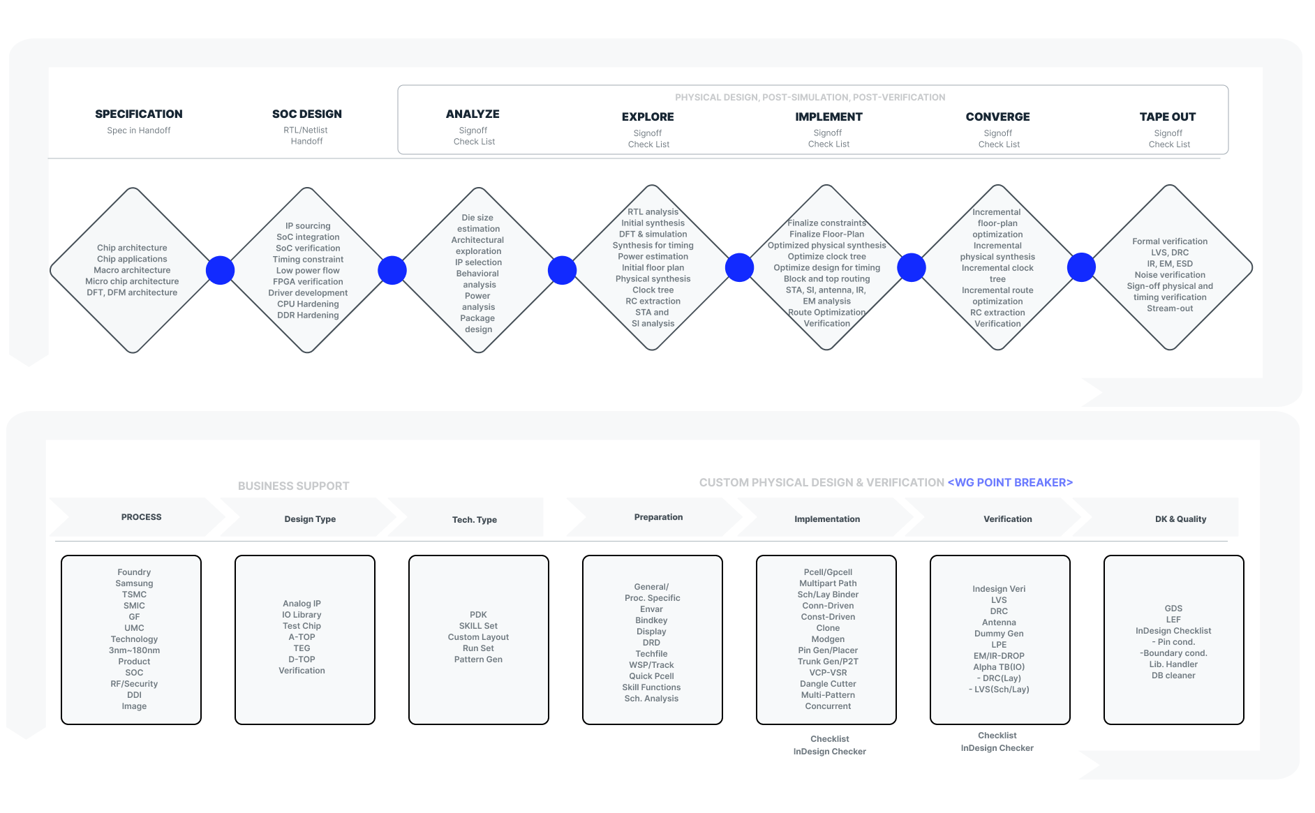
FULL CHIP DESIGN
Design / Verification Platform System Architecture Analysis Power Management Control Real Emulation with FPGA IP Supplier Partnership Device Driver, BSP, OS porting
PHYSICAL IMPLEMENTATION
DFT (SCAN / BIST / JTAG) In-system Test STA (Static Timing Analysis) Synthesis & Timing Closure
PHYSICAL DESIGN
Full Chip Floor Plan Hierarchical Physical Design Low Power Design SI Check (IR Drop, Crosstalk-Noise)
PKG & TEST Develop
Package Design Test vector generation ATE test set-up Qualification & Reliability Q.A & Failure analysis
Mass Production
Wafer Business Full Turn-key Business (Wafer + PKG + TEST)
PHYSICAL DESIGN
Test부터 양산 생산/공급까지 빠른 TAT를 달성하기 위하여 장기적이고 전략적인 파트너십 프로그램으로 업계 최고 grade의 공정 및 PKG / Test 기술의 성공적인 case study를 쌓음으로써 고객에게 전체 Process에 걸쳐 Total Solution을 제공합니다
Advanced Technology


